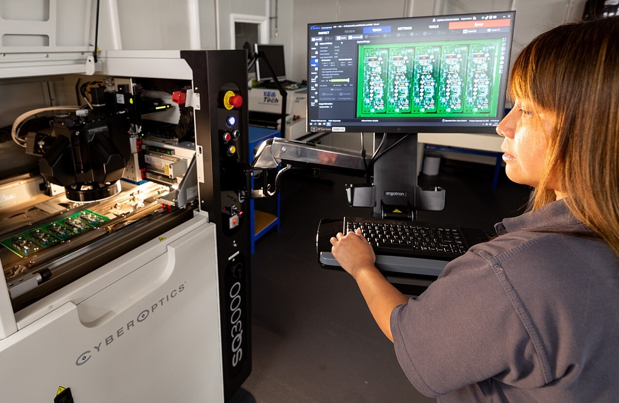
Home » News » Stage 4: PCB Plate, Strip & Etch

Stage 4: PCB Plate, Strip & Etch

The now developed board will continue through the next phase which includes; copper and tin plating, resist stripping, etching and tin stripping

Copper and Tin Plating

The developed panel can now be passed through the electrolytic plating process. This process plates a controlled amount of copper into the metallised holes and onto any exposed copper features (tracks and pads) forming the electrical interconnections between top, bottom and internal copper layers to ensure circuit functionality. The photo-resist which remains on the panel from the previous process acts as a template for the circuit features to plate onto and in addition prevents the copper and tin from plating onto any areas where they are not required. The tin is used as an etch resist and is important in ensuring that the track and pad definitions are maintained during the later stage etch process.

Resist Strip

Once the panel has been plated the photo-resist is no longer required and can be stripped from the panel. This is done in a horizontal process containing a pure alkaline solution which efficiently removes the photo-resist leaving the base copper of the panel exposed for removal in the following etching process.

Etching

The etching process is also a controlled horizontal process and efficiently removes all unwanted copper from the PCB panel using a highly aggressive Ammonia based solution. As the plated copper tracks and pads are covered and protected by the tin which is resistant to the etching chemistry, all that is left on the panel after the etching process is the layout of the circuit design in copper with a tin covering which now forms the basis of a functioning PCB.

Tin Stripping

All that remains is to remove the plated tin, this is also carried out in horizontal processing equipment. The tin is removed using a concentrated Nitric acid based solution which is highly effective at removing the tin metal without attacking the circuit copper underneath. We are now left with a defined copper outline of the PCB design which is ready to be passed through to the next process – Solder Resist Dept.